[ad_1]

The biggest change, according to Gelsinger’s comments via The Register, is moving away from the notion that foundries just produce wafers. Instead, he sees this service evolving into providing an entire “system” for clients. That system includes providing the wafer along with multiple tiles, advanced packaging, and software to tie it all together. To describe this evolution, Gelsinger says it will be providing System on Package, or SOP for short. Describing a rack in a data center, Gelsinger explained, “when I say the rack is becoming a system, the system is becoming an advanced chiplet-based SOP, that’s exactly what we mean and how we see it evolving.”

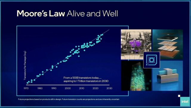
Intel’s vision for the increase in transistor density over the course of the next eight years. (Image: Intel)
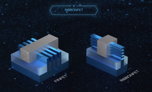
Part of this evolution involves shrinking nodes along with die-stacking, which Intel has previously discussed. In 2024 Intel will give up FinFET and move to gate-all-around (GAA) RibbonFET transistors. This will be its 20A node, as Intel ditches the nanometer nomenclature for Angstroms. At the same time, it’s also introducing PowerVIA, which is backside power delivery. Gelsinger believes this shift along with packaging advances will pave the way for unbridled advancements in semiconductor density.
“Today, there are about 100 billion transistors on a package, and we see our way clear to getting to a trillion transistors by the end of the decade,” he said. “With ribbon FET we have a fundamental new transistor structure that we’re just about to come into, that we believe continues to scale through the end of the decade.”

Gelsinger also believes the mix-and-match technology it’s using for Meteor Lake is the future. That means combing different chips, or tiles, built on different nodes based on what’s the most efficient. As an example, Meteor Lake will combine four different process nodes across both its own foundry and TSMC’s. It will be building the base interposer on its 22nm process, and the CPU tile on Intel 4 (previously 7nm). Meanwhile, TSMC will be making the SoC, I/O, and GPU on its own N5 and N6 processes.
“You may say, hey, I’m getting two chiplets from Intel, I’m getting one of the chiplets from a TSMC factory, maybe the power supply components from TI, maybe there’s an IO component coming from Global Foundries, and of course, Intel has the best packaging technologies so they’re gonna be the one assembling all those chiplets together, but maybe it’s another assembly provider as well, so we do see that mix and match happening,” Gelsinger said.

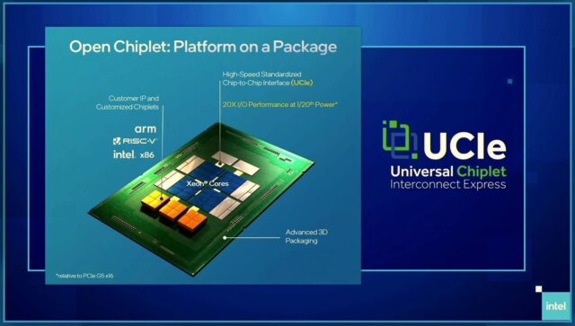
Gelsinger is likely correct about packaging becoming the dominant advantage one foundry has over another. As die shrinks become less frequent and chiplets move to the forefront, how those pieces go together will be crucial technology in the years to come. To that end, Gelsinger also touted its universal chiplet connector based on PCI Express. It’s aptly named, you guessed it, Universal Chiplet Interconnect Express (UCIe). This is an Intel-led consortium that seeks to standardize the mixing and matching of chiplets from various foundries. It includes some of the biggest names in the semiconductor world, including AMD and Qualcomm. Notably missing are Apple and Nvidia.
Whether this will be a winning strategy for Intel remains to be seen. We will find out soon enough though, as Intel confirmed Meteor Lake is on-target for 2023 at the same conference. This will be the company’s first “disaggregated” chip design, featuring the aforementioned tiles from two different foundries. As an aside, this mixing-and-matching was supposedly the cause of rumored delays for Meteor Lake, which reveals a flaw in the strategy. If some tiles are being made on advanced nodes, and they’re not all ready at the same time, problems arise. Intel has denied those rumors and says it’s still on schedule.
Now Read:
[ad_2]
Source link
