
[ad_1]
Discover how IoT is changing the game for PCB design and functionality, and why this will not doubt evolve as business applications expand.
One of the mega-tech trends revolutionizing today’s digital world is the ubiquitous Internet of Things (IoT). The significant factors pushing the IoT market are the decreased CPU memory and storage cost, abundant availability of sensor devices, and accessibility of expandable repositories for storing data (like cloud service). IoT devices can track, monitor, control, and optimize information about a product. These features indicate the long-term impact of IoT in applications like smart farming, connected vehicles, smart grids, and many more.
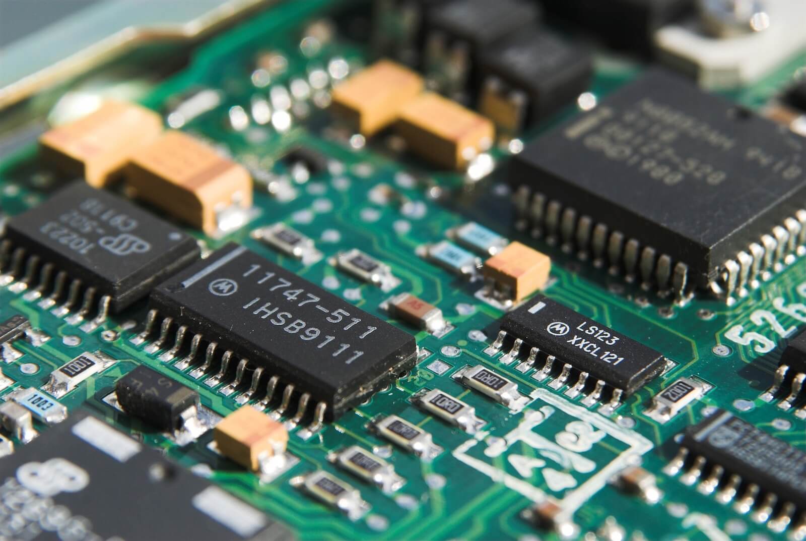
The design of an IoT device depends on the precise selection of the sensors, wireless connecting network, and power management. The traditional PCB design methods may not support the functionalities offered by an IoT product. Wearable IoT devices like fitness trackers or smartwatches are supposed to be smaller in size but with full-packed features. For example, a smartwatch has to include a clear display, multiple sensors, a microcontroller, a Bluetooth chip for communication, and a battery. A PCB in such an application is expected to be very tiny, yet reliable.
In industrial IoT applications, the requirements are even more stringent as most of these devices are expected to be online and transmit information without downtime. The PCB design in these applications should focus on effective power management.
Most IoT devices are designed to operate in a moving environment with resistance from the external setting. Conventional routing techniques are not suitable for this application. A combination of Flex and HDI PCB is used to develop tiny, lighter, and faster IoT devices.
Fabricating Flex PCBs for IoT is quite different and demands accurate measurement of bend ratio, signal trace thickness, copper weight, heat generation of the components, and lifecycle repetitions. Thus, the PCB development and fabrication processes continuously upgrade to meet the IoT market requirements.
Design requirements impacting the future of PCBs in a world driven by IoT applications:
The substrate material of an IoT PCB should be flexible and lightweight. Flex PCBs and HDI PCBs are extensively used in this application. Flexible PCBs are best suited for wearable devices as more components can be placed in a small area. The wiring is simplified by HDI PCBs along with minimal mechanical stress.
The compact design requirements demand a thorough simulation and virtual prototyping to incorporate the design shape in the intended form of the IoT device. The necessity of miniaturized components has increased largely, and many latest sensors are manufactured using MEMS (Micro electro-mechanical systems) technology to offer small footprints with high reliability. Future IoT designs may favor a new approach where mechanical and electrical circuit changes can be done concurrently.
IoT applications have eliminated the luxury of space for designers in component placement and routing. Multilayer PCBs are designed with strict EMC regulations. The peak component density and an increased count of vias in the circuit are achieved using HDI PCBs. The integrity of the sensor signals must be ensured by eliminating any possible coupling and interference issues in the design.
The component packages can not be through-hole or surface-mount types in IoT design. So, there’s no possibility for through-hole or SMT PCB Assembly. The miniature gadget size has resulted in the development of new package technologies like multi-chip modules (MCM), system-in-package (SiP), and three-dimensional Integrated circuits (3D-ICs).
One of the critical requirements of an IoT device is the extended battery life. Designers should choose the right power management integrated circuits (PMIC) and calculate the power budget for each functional block. Power consumption varies according to the operating state of the device, and hence analyzing all corner cases is important during power estimation. The battery life drains faster in applications like health care monitoring devices, wireless transceivers, etc, which have a continuous activity involved. Techniques like energy harvesting and design compliance with wireless standards can improve power efficiency and battery life.
As IoT devices are connected to a shared network, a security breach is an apparent possibility. There are applications involving sensitive data like medical details or financial information which can be misused. Along with software security updates, there is an increasing need for hardware protection in IoT devices.
Another vital feature required in IoT devices is their adaptability to end-user interaction. The human body temperature, moisture, and mobility can affect the performance of an IoT device, especially in wearable products. Simulating these conditions during the design stage and implementing suitable compensation circuits are important in an IoT PCB design.
Manufacturing requirements for IoT PCB:
Involving the contract manufacturer from the design stage itself is recommended for an effective PCB fabrication for your IoT device. Flexible PCBs and components in SiP packages can simplify the fabrication process. Preventing the usage of counterfeit components and adding identification codes in each layer of the PCB can improve the security of the IoT circuit.
It is necessary to consider the potential issues during the design to avoid failures after deployment. Generally, IoT devices are classified as consumer, industrial and enterprise devices. The DFM requirements of a consumer IoT device (like smart TV, and wearable devices) are a balanced stack-up, managing connector constraints, and selecting the PCB material with the required bend ratio.
Industrial IoT devices (like Motors, and construction vehicles) should have high board strength, thermal capacity, and high voltage. Including enough thermal relief during layout design is recommended for better PCB performance.
Enterprise IoT devices (like security systems, and computing devices) demand high power reliability, high-frequency/RF connectivity, etc. The ease of depanelization and enough spacing for component rework can improve manufacturability.
Wrapping Up
With IoT devices, we can collect data and use this information to build customized products. Combining IoT with 3D electronic printing technology has a tremendous potential to speed up the manufacturing process and can also build 3D PCBs. An optimized IoT PCB can be used in healthcare, aeronautics, defense, and many other applications. The PCB design for IoT applications may become more specific as the business expands. New features can bring new challenges, but there are a common set of requirements indicating a possibility of using similar design procedures frequently.
[ad_2]
Source link